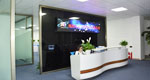
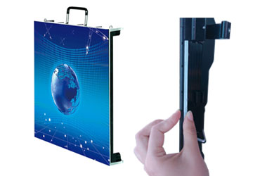
From:Small spacing gaoqingbing suppliers Edit:Shenzhen Xmedia Technology Co.,Ltd
As for today, white light LED still has the poor luminescence uniformity and the life of the sealed materials is not long, and can not play the advantages of white LED is expected to be applied. But on the demand level, not only the general lighting purposes, with the wide application of LCD mobile phone, TV, car and medical treatment actively, make the most appropriate development of stable white light LED technology research is quite concerned.
Increasing the amount of light by increasing the area of the wafer
In order to improve the luminous efficiency of white LED, there are two directions, is to improve the LED chip area, that is to say, the area of 1m square meters of small chip, the luminous area increased to 10m square meters above, to increase the amount of light, or put a few small chips packaged together in the same model.
Although the area of the LED wafer is large, it can achieve much higher brightness, but because of too large area, the application process and results will backfire. Therefore, in order to solve this problem, some LED operators can improve the luminous efficiency of 50lm/W according to the improvement of electrode structure and the structure of cladding, which is improved on the wafer surface.
For example, in white LED flip chip package, because near the light emitting layer is very close to the package, the light emitting layer to outside the shed, so the electrode is not obscured by the advantages, but the disadvantage is not easy to dissipate the heat generated by the.
Instead of the wafer surface is improved, coupled with the increase in chip area is absolutely can really improve the brightness, because when the light scattering from the wafer inside out, these improvements can not be reflected in part of the wafer, so the light will be a limit, according to the calculation, the best light efficiency is LED chip size in about 7m square meters.
Rapid improvement of luminous efficiency by encapsulating several small area LED wafers
Compared with the large area of LED chip, with a small power module by using LED chip package, which is able to meet the requirements of high brightness, for example, Citizen will be 8 small LED package together, let the module luminous efficiency reaches 60lm/W, which is the industry''s first.
But this approach also led to some doubts, because is an LED package in the same module, so the module must be placed into some insulating materials, so as to avoid the occurrence of short circuit between the LED chip, however, this way will increase the cost of many.
This Citizen explained that in fact to affect the rate of cost is very small, because compared to the overall proportion of the cost, the insulating material is only one percent or less, and because you can use the existing material for insulation applications, these insulating materials do not need to develop, also do not need to add new equipment to cope with.
Although the explanation of Citizen is reasonable in theory, it is a challenge for the inexperienced industry, because it needs to be overcome in the aspects of yield, R & D and production engineering.
Of course, there are other ways to improve the luminous efficiency of the target industry, many researchers found that produce structure of concave and convex uneven in LED sapphire substrate, it can increase the light output, therefore, has gradually towards the establishment of Texture or Photonics crystals on the surface of the wafer structure.
For example, Germany''s OSRAM is the development of such a framework "Thin GaN" high brightness LED, OSRAM is formed on the InGaN layer of metal film, and then spin off the sapphire. In this way, the metal film will produce the mapping effect and obtain more light extraction, and according to the OSRAM data, this structure can achieve 75% of the light extraction efficiency.
Gradually the industry is constructed using flip chip, to expect to achieve the luminous efficiency of 50lm/W, due to the nearby light emitting layer is very close to the package, the light emitting layer to outside the shed, so the electrode can not be shaded.
Of course, in addition to the wafer light extraction needs to work hard, because the expected to achieve higher light efficiency, in the package part also have to do some improvement. In fact, every increase of a project will be on the light extraction efficiency, bring some impact, but this does not mean that, because the packaging process will increase the loss of light is higher, as the Japanese plane light source technology developed by OMROM, can greatly improve the light extraction efficiency, the structure of OMROM this is the LED rays, to control by using LENS optical system and optical system, so OMROM called "Double reflection" optical system.
With this structure, the light loss of traditional shell type package LED the package for the wide angle reflection to obtain higher light efficiency, further more, the processing surface of the formed Mesh, and the formation of double reflection effect, this way, in fact you can get a good light extraction efficiency control. Because of this special design, these reflective effects to achieve high light extraction efficiency of LED, the main purpose is for LCD TV backlight applications.